Circuit Examples
This page contains a few worked examples of creating truth tables from circuits. It is important to work through a circuit carefully, avoiding the temptation to take shortcuts in an attempt to finish quickly. Rushing often leads to using incorrect shortcuts, which makes the resulting truth table wrong.
Video Lecture
Be Careful with NOT
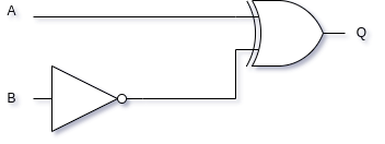
The presence of a NOT gate definitely changes the operation of a circuit. However, its location determines its effect. Consider the following circuit, which has a NOT gate on one of the inputs:
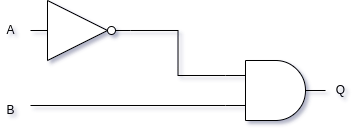
In constructing a truth table for the circuit in Figure 1, it might be tempting to look at the Common Gates and pick the truth table for a NAND gate. However, taking that shortcut would result in the wrong answer. Instead, trace the circuit by hand to generate the following truth table:
| A | B | Q |
|---|---|---|
| 0 | 0 | 0 |
| 0 | 1 | 1 |
| 1 | 0 | 0 |
| 1 | 1 | 0 |
Look back at the truth table for a NAND gate. Notice that the truth table in Table 1 does not match the truth table for a NAND gate. Therefore, it can be said for certain that the circuit A·B is not the same circuit as A·B.
Let’s see what happens when we move the NOT gate to the output side of the AND gate. This is done in Figure 2.
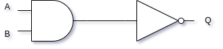
Once again, we can trace the circuit and complete its truth table:
| A | B | Q |
|---|---|---|
| 0 | 0 | 1 |
| 0 | 1 | 1 |
| 1 | 0 | 1 |
| 1 | 1 | 0 |
Now, compare Table 2 to the truth table for NAND. These match, so placing a NOT gate on the output side of an AND gate does create a NAND gate. However, placing the NOT gate on the input side of an AND gate does not create a NAND gate. The key here is to recognize the location of the NOT gate: is it on the input side, or is it on the output side?
The same principle applies when mixing a NOT gate with an OR gate. A NOR gate is created only when the NOT gate is on the output side of the OR gate.
Look for the NOT Circle
So why do we have NAND and NOR gates, if we can just put a NOT gate on the output side of an AND or OR gate? The answer has to do with cost and performance: we can manufacture NAND and NOR gates in such a way that one NAND or one NOR gate can be slightly less expensive than an AND or OR gate plus a NOT gate. While the savings is tiny for a single gate, remember that there can be billions of gates inside a computer system, and computers are found everywhere. Therefore, tiny cost savings can add up at scale.
A second reason to use NAND and NOR instead of separate NOT gates concerns performance. When two gates are wired together, such that the output of one gate is connected to the input of another gate, it takes slightly longer for the output of the second gate to stabilize whenever the inputs change. This phenomenon is called propagation delay, and too much of it within a system can have a measurable performance impact.
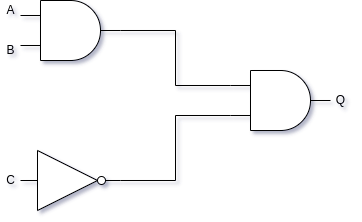
For these reasons, we have NAND and NOR gates (and XNOR gates). The key to distinguishing these gates is to look for the tiny circle on the output side of the gate. That little circle logically says the same thing as wiring a NOT gate to the output of the base gate (AND, OR, or XOR). Let’s see an example of a circuit using NAND and NOR:
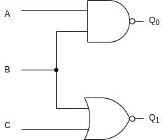
The circuit in Figure 3 looks a little more complicated than the circuits we’ve seen so far. However, it isn’t that difficult to trace, if we look at what the circuit is doing. Here we have 3 inputs: A, B, and C. We also have two outputs: Q0 and Q1, which correspond to the outputs of a NAND and NOR gate, respectively.
On the input side, input A connects only to the NAND gate. Input C connects only to the NOR gate. However, input B is a little different. It connects to a small black dot, which then connects to both the NAND and NOR gates. The small black dot indicates a connection between wires. Therefore, the input signal B is wired to both the NAND and NOR gates.
Logically, the NAND gate implements the circuit A·B. The NOR gate implements the circuit B+C. Since the outputs of the two gates correspond to our two outputs, we can effectively trace this circuit as two different sub-circuits.
| A | B | C | Q0 | Q1 |
|---|---|---|---|---|
| 0 | 0 | 0 | 1 | 1 |
| 0 | 0 | 1 | 1 | 0 |
| 0 | 1 | 0 | 1 | 0 |
| 0 | 1 | 1 | 1 | 0 |
| 1 | 0 | 0 | 1 | 1 |
| 1 | 0 | 1 | 1 | 0 |
| 1 | 1 | 0 | 0 | 0 |
| 1 | 1 | 1 | 0 | 0 |
To compute the truth table shown in Table 3, it is easiest to compute each output separately. Output Q0 is the output of the NAND gate in A·B. Therefore, this output will be 1 on almost all rows. It will be 0 only on those rows where both A and B are 1, since this is the meaning of a NAND gate.
A NOR gate only turns on when both its inputs are 0, since it is the opposite of an OR gate. For the output of the NOR gate in our circuit (Q1), we can fill in zeroes everywhere that both B and C are not zero. The NOR gate only outputs 1 on the two rows where B and C are both 0.
Using a similar circuit tracing strategy, you can compute the truth table for any logical circuit. All you need to do is dedicate enough time, work carefully, and refer to the truth tables of the common gates to use as building blocks.
Practice Problems
Try working these problems yourself before revealing the answers.
- Construct a truth table for the following circuit:
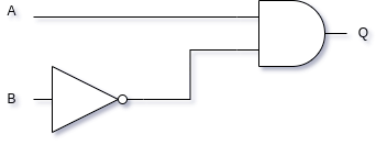
Show Answer
The logical expression for this circuit is A·B. Notice that the NOT gate is on the input side of the circuit, so you cannot simply replace the whole circuit with a NAND gate.
| A | B | Q |
|---|---|---|
| 0 | 0 | 0 |
| 0 | 1 | 0 |
| 1 | 0 | 1 |
| 1 | 1 | 0 |
- Construct a truth table for the following circuit:
Show Answer
The logical expression for this circuit is A⊕B.
| A | B | Q |
|---|---|---|
| 0 | 0 | 1 |
| 0 | 1 | 0 |
| 1 | 0 | 0 |
| 1 | 1 | 1 |
For two inputs, it so happens that this circuit is replaceable by an XNOR gate. There are gates that work with more than two inputs, which we have not covered in this course. Consequently, this observation does not generalize beyond two inputs.
- Construct a truth table for the following circuit:
Show Answer
The logical expression for this circuit is A·B·C.
| A | B | C | Q |
|---|---|---|---|
| 0 | 0 | 0 | 0 |
| 0 | 0 | 1 | 0 |
| 0 | 1 | 0 | 0 |
| 0 | 1 | 1 | 0 |
| 1 | 0 | 0 | 0 |
| 1 | 0 | 1 | 0 |
| 1 | 1 | 0 | 1 |
| 1 | 1 | 1 | 0 |
If you had trouble tracing this circuit, break down the problem, and start by figuring out what the first AND gate does. It can only produce a 1 if both A and B are 1, a combination that occurs only in the last two rows of the truth table. On those two rows, the second AND gate can only produce a 1 whenever C is 0, due to the NOT gate between C and the second input to the second AND gate. Therefore, only row 110 of the table can produce an output (Q) of 1. All the other rows will output 0.
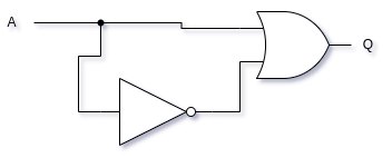
- Construct a truth table for the following circuit:
Show Answer
This circuit represents A+A.
| A | Q |
|---|---|
| 0 | 1 |
| 1 | 1 |
Whenever A is 0, the second input to the OR gate is 1 (since is 1). An OR gate produces an output of 1 whenever either (or both) of its inputs is 1. Therefore, this circuit always produces an output of 1.
This circuit is an example of a tautology and can be replaced with a wire connected to VCC.
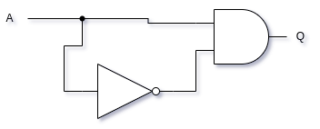
- Construct a truth table for the following circuit:
Show Answer
This circuit represents A·A.
| A | Q |
|---|---|
| 0 | 0 |
| 1 | 0 |
Whenever A = 0, A == 1. Whenever A = 1, A == 0. Therefore, one side of this AND gate is always going to be receiving a zero, causing its output to be 0 for either input value.
This circuit is an example of a fallacy and can be replaced with a wire connected to GND.
