Introduction to the CPU
The Central Processing Unit (CPU) is the “brain” of the computer system. It is the component that carries out computation and controls the rest of the computer. To understand how the CPU operates, we start by looking at its fundamental design, or its architecture. At a high level, the architecture of the CPU describes what functions it performs and how it goes about performing those functions. From the middle part of the 20th century, two major high-level architectures emerged: the von Neumann Architecture and the Harvard Architecture. Both of these architectures influenced the design of the current generation of microprocessors.
Video Lecture
The von Neumann Architecture
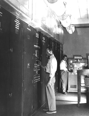
Sometimes also called the Princeton Architecture, the von Neumann Architecture (“von-noy-mahn”) describes the design of the Electronic Discrete Variable Automatic Computer (EDVAC)1, which was constructed using 3,563 vacuum tubes, occupied 490 square feet of floor space, weighed 17,300 pounds, and drew 50,000 Watts of power (plus an additional 25,000 Watts for its dedicated air conditioner).2 Depicted in Figure 1, this computer was divided into several logical parts:
- The central arithmetic (CA) part, which is responsible for performing mathematical calculations.
- The central control (CC) part, which ensures that instructions are carried out in the proper order.
- The memory (M), which holds the intermediate results of a computation, the instructions to be carried out, and other information.
- Some method for transferring input into the control parts (CC and CA) and memory.
- Some method for recording the output information from the control parts and memory, once the computation is finished.

Although the EDVAC eventually went the way of the vacuum tube, the compartmentalization of components as documented by von Neumann is still present in modern computers. The original CA and CC components are part of the CPU in a modern system, while the memory is found in various different parts of a modern computer (including inside the CPU in the form of registers and cache storage). We still view input and output devices as distinct components, although punched paper tape and line printers have given way to keyboards and screens.
From the perspective of CPU design, the key contribution of the von Neumann Architecture is that the machine instructions to run the programs are stored in the same memory as the data upon which the programs will operate. This architecture simplifies the design of the computer by requiring only a single memory controller to be able to load both instructions and data.
Harvard Architecture
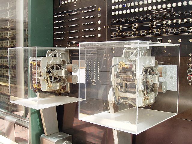
The main “competing” architecture to the von Neumann Architecture is the Harvard Architecture, which was developed for the Harvard Mark I computer, commercialized as the IBM Automatic Sequence Controlled Calculator (ASCC). Unlike the EDVAC, which was fully electronic (albeit with the use of tubes), the ASCC was an electromechanical computer. It was described as “light weight” with compact dimensions of merely “51 feet long and 8 feet high.” Moreover, “[w]hen in operation in the soundproofed Computation Laboratory, the calculator is so light and so finely geared that it makes no more noise than a few typewriters.”4

Unlike the EDVAC, the Mark I used a separate “sequence control tape”4 to contain the computing instructions. Data were fed into and out of the machine using a separate tape mechanism (see Figure 2). As a result, the computational instructions and data in the Harvard Architecture are stored in separate memories, isolated from one another. Contrast this approach with the von Neumann Architecture, which stores the instructions and data together in the same memory.
In practice, modern computer systems largely utilize a hybrid of the von Neumann Architecture and the Harvard Architecture (sometimes called the Modified Harvard Architecture). The same memory access mechanisms are used to store both the instructions and data, as is the case with the von Neumann Architecture. However, for performance reasons, the instructions are routed separately within the CPU, going into separate caches from which the CPU pulls instructions separately from the data. In addition, the CPU may implement certain access control mechanisms to prevent execution of instructions that are loaded from purely data regions of storage, improving protection from malware.
Microprocessors
Unlike the EDVAC and Mark I, which required dedicated facilities unto themselves, modern computer systems are much smaller. This shrinkage is due to our ability to manufacturer processors (and other computer components) that fit onto a single silicon chip. Each individual circuit in such a microchip is microscopically small, enabling extremely large numbers of circuits to be packed densely onto the chip.
Although the size and power consumption of the modern microprocessor (a processor on a microchip) are greatly reduced from the EDVAC and Mark I, the principles by which modern CPUs operate remain the same. CPUs read their machine instructions from memory, generally using the same memory access mechanisms for both the instructions and the data. Standardization of the underlying hardware permits collections of machine instructions to moved from system to system as if they were ordinary data, creating the notion of software.
Notes and References
-
Michael D. Godfrey. “First Draft Report on the EDVAC by John von Neumann.” IEEE Annals of the History of Computing 15(4): 27-43, 1993. Article on ResearchGate ↩
-
Martin H. Weik. “A Survey of Domestic Electronic Digital Computing Systems.” Ballistic Research Laboratories Report No. 971. December, 1955. Archived by Ed Thelen: EDVAC ↩
-
Image Credit: United States Army (via Wikimedia Commons). License: Public Domain. ↩
-
IBM. “ASCC General Description.” IBM Archives ↩↩
-
Image Credit: Daderot (via Wikimedia Commons). License: CC-BY-SA. ↩
